Semiconductor
Motion Solutions has a long history of providing automation components, engineered solutions, and manufacturing services to the semiconductor industry.
Companies in this sector bring value more through incremental performance improvements for a reasonable price than through innovation. Motion Solutions has decades of experience developing systems that meet the needs of these types of applications. Take advantage of our laboratory automation system knowledge to get better products to market faster.
Clean Room Assembly Expertise
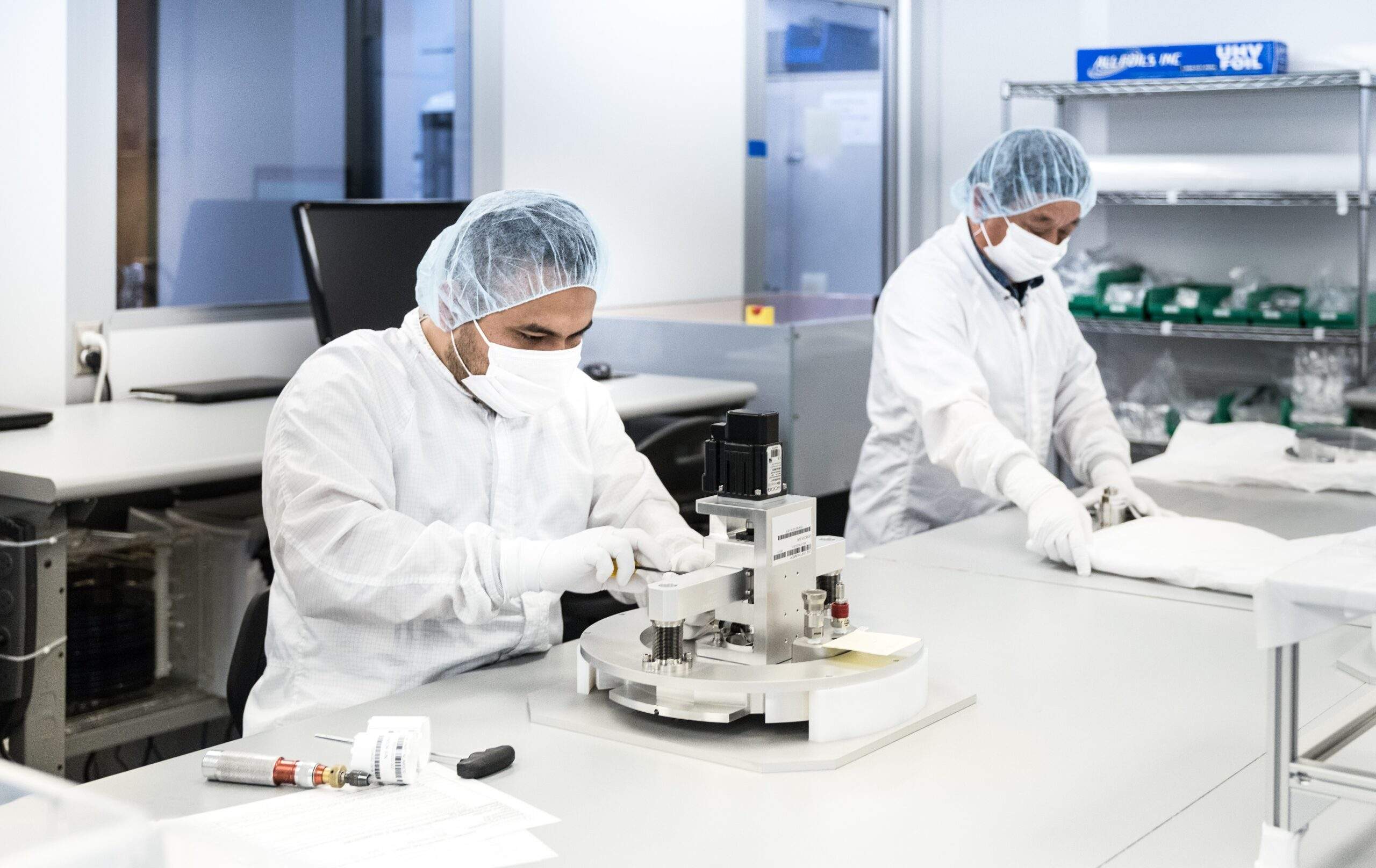
Clean assembly is a particular field that calls for specialized procedures, equipment, and environmental controls. Precision-cleaned surfaces could be impacted during the assembly process if tools and worker contact are not strictly controlled.
Clean Room Motion System Design
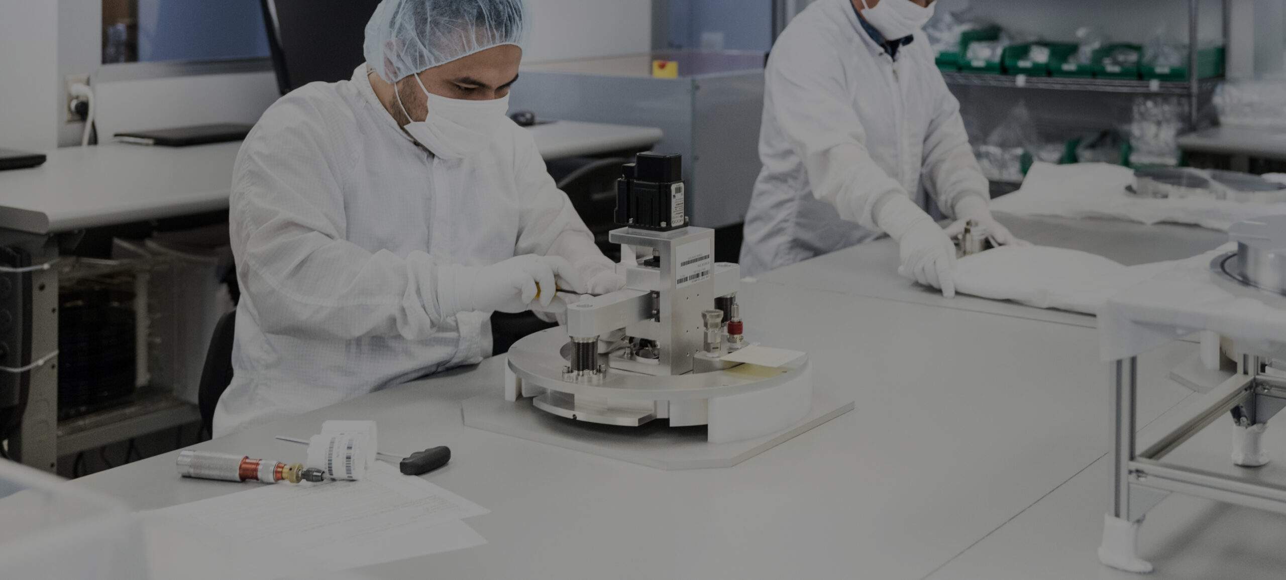
Our class-1000 clean room enables us to support high-precision motion control projects for semiconductor, aerospace, and other similarly demanding industries. This controlled environment equips us to tackle contamination-sensitive assemblies.
High Vacuum Positioning Systems
Vacuum applications are typical in manufacturing semiconductors, liquid crystal displays, plasma displays, and fiber optics in areas where linear motion systems are used.
Helium Leak Detection
Several test facilities are devoted to making sure that every product that leaves the building operates to its full potential. A helium leak detector from our specialized equipment checks vacuum seals. Gas and vapor emissions impact vacuum environments and make it more difficult to achieve or maintain the necessary vacuum level. Verification testing validates that the design complies with requirements.
Clean Room Packaging and Handling
It’s crucial to obtain, fabricate, assemble, test, package, and ship semiconductor parts without causing any damage. Our knowledgeable staff has years of training and experience in successfully managing this process from prototype to production.
Vacuum/ Clean Room Bearing Preparation
Bearings must be correctly designed, cleaned, and pre-loaded to reduce particle formation. We completely clean bearings using our recirculating ultrasonic vapor degreaser and re-grease them to clean room standards.
Industry Challenge
Semiconductor equipment vendors and end-users face significant challenges. Positioning equipment needs to operate to micrometer-scale accuracies and sub- micron tolerances. Many of the processes used to fabricate ICs are performed under vacuum conditions. As a result, control of particulates and contamination is crucial. Even outside of the vacuum environment, a few parts per million of particulates can dramatically reduce yield. Semiconductor process steps frequently take place at high temperatures, which requires specialized materials and lubrication. Equipment may require active cooling, as well.
The Motion Solutions Advantage
At Motion Solutions, we have a track record of working with semiconductor equipment vendors who built top tier semiconductor diodes, sensors, and other automation equipment. Our primary production floor features a class-1000 clean room with a class-100 laminar flow bench. We have specialized cleaning equipment and protocols in place to control contamination. In addition, our engineering team is well-versed in the nuances of designing equipment to operate in vacuum and at high temperatures. These techniques include the use of specialized materials, coatings, and lubricants. We have a helium-leak detector that equips us to test vacuum devices. Similarly, we can evaluate the performance of water-cooled equipment using pressurized circulating water to confirm designs are leak-proof.
To minimize particle generation, bearings need to be properly designed, fabricated, and run in. Even the structure of the equipment and its alignment comes into play. Equipment like semiconductor sensors and diodes requires class A finishes free of tool marks, scratches, and abnormalities that might generate particulates. Procuring, fabricating, assembling, testing, and shipping semiconductor parts without damaging them is both critical and extremely challenging. Our expert staff has years of training and experience in managing this process successfully.
Proven Solutions
One of the difficulties with contamination control in semiconductor equipment is that the bearings and guides used to support motion generate particles when they are first manufactured. As a result, they need to be run in before use in a semiconductor process environment. Industry practice is to lubricate bearings at the factory, then send them to the customer for run in. The problem is that the particles then remain in the lubricant. This can either cause running performance problems or premature wear. For select, critical situations, we run in the bearings, remove the lubricant, then clean the bearings thoroughly with our recirculating ultrasonic vapor degreaser. We reassemble the now-immaculate device for final acceptance testing and shipment.
Bearings aren’t the only semiconductor components that can cause contamination. If a wafer slips in a wafer-handling robot, at best it will catastrophically alter the patterning. At worst, it will slip out of the handling robot and break. At this point, the process chamber/equipment needs to be thoroughly cleaned, which can lead to days of downtime. We test our wafer-handling robots with a custom fixture that monitors wafer positioning for slippage. This equipment enables us to fine-tune our designs and perform acceptance testing on every device that goes out the door.
